Softening of nanocrystalline metals at very small grain sizes
Jakob Schiøtz, Francesco D. Di Tolla and Karsten W. Jacobsen
Center for Atomic-scale Materials Physics and Department of
Physics, Technical University
of Denmark, DK-2800 Lyngby, Denmark
-
Present
address: SISSA, Via Beirut 2-4, I-34014 Grignano (TS),
Italy.
This paper was published in
Nature
vol. 391 p. 561 (5 Feb
1998)
Nanocrystalline solids, in which the grain size is in the nanometre
range, often have technologically interesting properties such as
increased hardness and ductility. Nanocrystalline metals can be
produced in several ways, among the most common of which are
high-pressure compaction of nanometre-sized clusters and high-energy
ball-milling.[1,2,3,4] The result is a polycrystalline metal
with the grains randomly orientated. The hardness and yield stress of
the material typically increase with decreasing grain size, a
phenomenon known as the Hall-Petch effect.[5,6] Here we present computer simulations
of the deformation of nanocrystalline copper, which show a softening
with grain size (a reverse Hall--Petch effect[7,3]) for the smallest
sizes. Most of the plastic deformation is due to a large number of
small 'sliding' events of atomic planes at the grain boundaries, with
only a minor part being caused by dislocation activity in the grains;
the softening that we see at small grain sizes is therefore due to
the larger fraction of atoms at grain boundaries. This softening will
ultimately impose a limit on how strong nanocrystalline metals may
become.
To simulate the behavior of nanocrystalline metals with the computer,
we construct nanocrystalline ``samples'' with strucures similar to
what is observed experimentally: essentially equiaxed dislocation-free
grains separated by narrow straight grain boundaries[1]. Each
sample contains 8 to 64 grains in a 10.6nm cube of material,
resulting in grain sizes from 3.3 to 6.6 nm. The grains are produced
by a Voronoi construction:[8] a set of grain centers are
chosen at random, and the part of space closer to a given center than
to any other center is filled with atoms in an fcc (face centered
cubic) lattice with a randomly selected crystallographic orientation.
A typical ``sample'' is shown in Fig. 1a. To
mimic that the system is deep within the bulk of a larger sample, the
system is replicated infinitely in all three spatial directions
(periodic boundary conditions). The forces between the atoms are
calculated with the Effective Medium Theory,[9,10]
which suitably describes many-atom interactions in metals. The metal
chosen for these simulations is copper, very similar results were
obtained with palladium. Before deforming the system we ``anneal'' it
by running a 50ps molecular dynamics simulation at 300K, allowing
unfavorable configurations in the grain boundaries to relax. Doubling
the length of the annealing does not have any significant effect, nor
does an increase of the temperature to 600K.
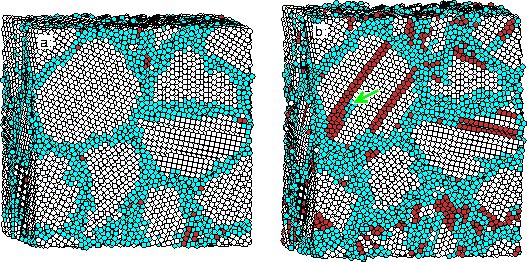
Figure 1:
A nanocrystalline copper sample (a) before and (b) after 10%
deformation. The system contains 16 grains and approximately
100000 atoms, giving an average grain diameter of 5.2 nm. Atoms
in the grain boundaries are colored blue, atoms at stacking faults
are colored red. We clearly see stacking faults left behind by
partial dislocations that have run through the grains during the
deformation processes. Such stacking faults would be removed if a
second partial dislocation followed the path of the first, but
this is not observed in the present simulations. In the left side
of the system a partial dislocation on its way through a grain is
seen (green arrow).
 |
The main part of the simulation is a slow uniaxial deformation while
minimizing the energy with respect to all atomic coordinates. The
deformation is applied by expanding the simulation cell in one
direction, while the size is allowed to relax in the two perpendicular
directions.
The initial and final configurations of such a simulation with a total
strain of 10% are shown in Fig. 1. We see how
the grain boundaries have become thicker, indicating that significant
activity has taken place there. In the grains a few stacking faults
have appeared. They are the signature of dislocation activity
within the grains.
To facilitate the analysis of the simulations, we identify which atoms
are located at grain boundaries and which are inside the grains, by
determining the local crystalline order.[11,12]
Atoms in local fcc order are considered ``inside'' the grains, atoms
in local hcp (hexagonal close packed) order are classified as stacking
faults. All other atoms are considered belonging to the grain
boundaries. Unlike conventional materials, where the volume occupied
by the grain boundaries is very small, a significant fraction
(30-50%) of the atoms are in the grain boundaries, in agreement with
theoretical estimates.[2]
While the deformation takes place, we calculate the average stress in
the sample as a function of the amount of deformation. For each grain
size the deformation of seven different initial configurations were
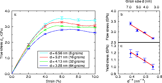
simulated. Fig. 2a shows the obtained average
deformation curves. We see a linear elastic region with a Young's
Modulus around 90-105GPa (increasing with increasing grain size),
compared to 124 GPa in macrocrystalline Cu[13]. This is caused
by the large fraction of atoms in the grain boundaries having a lower
Young's Modulus[14,15]. A similar reduction is
seen in simulations where the nanocrystalline metal is grown from a
molten phase[16]. The elastic region is
followed by plastic yielding at around 1GPa, and finally the plastic
deformation saturates at a maximal flow stress around 3GPa.
Figure 2:
a: The average stress versus strain for
each grain size. Each curve is the average over seven
simulations. The curves show the response of the material to
mechanical deformation. In the linear part of the curve (low
strains) the deformation is mainly elastic: if the tensile load is
removed, the material will return to the original configuration.
As the deformation is increased irreversible plastic deformation
becomes important. For large deformations plastic processes
relieve the stress, and the curves level off. We see a clear
grain size dependence which is summarized to the right. b
and c: The maximal flow stress and the yield stress as a
function of grain size. The yield stress decreases with
decreasing grain size, resulting in a reverse Hall-Petch
effect. The maximal flow stress is the stress at the flat part of
the stress-strain curves. The yield stress is defined as the
stress where the strain departs 0.2% from linearity.
 |
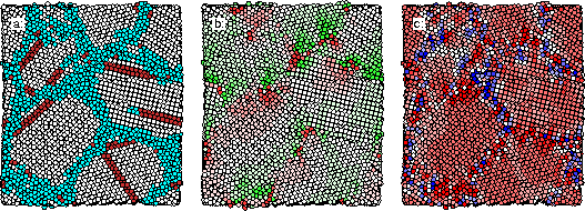
The main deformation mode is illustrated in Fig. 3b where
the relative motion of the atoms is shown. We clearly see that most
of the deformation occurs in the grain boundaries in the form of a
large number of small sliding events, where only a few atoms (or
sometimes a few tens of atoms) move with respect to each other.
Occasionally a partial dislocation is nucleated at a grain boundary
and moves through a grain. Such events are responsible for a minor
part of the total deformation, but in the absence of diffusion they
are required to allow for deformations of the grains, as they slide
past each other. No dislocation motion is seen in
Fig. 3, as none occured at that time of the simulation.
As the grain size is reduced a larger fraction of the atoms belongs to
the grain boundaries, and grain boundary sliding becomes easier. This
leads to a softening of the material as the grain size is reduced
(Fig. 2).
Figure 3:
Snapshot of grain structure, displacements and stresses at
8% deformation. (a) The position of the grain boundaries (blue)
and stacking faults (red) at this point in the simulation. (b)
The relative motion of the atoms in the z direction (up in the
plane of the paper) during the preceding 0.4% deformation. The
green atoms move up, red atoms move down. We see many small,
independent slip events in the grain boundaries, this is the main
deformation mode. (c) The stress field (the
 component) in the grains. Shades of red indicate tensile stress,
shades of blue compressive stress (dark colors corresponds to high
stresses). The stress in the grain boundaries is seen to vary
considerably on the atomic scale, and the average stress is
approximately 10-20% lower than in the grains.
component) in the grains. Shades of red indicate tensile stress,
shades of blue compressive stress (dark colors corresponds to high
stresses). The stress in the grain boundaries is seen to vary
considerably on the atomic scale, and the average stress is
approximately 10-20% lower than in the grains.
 |
The observed deformation mode is in some ways similar to the way grain
boundaries carry most of the deformation in superplastic
deformation.[17,18] The main difference is that in
superplasticity the grain boundary sliding is thermally activated,
whereas here it occurs at zero temperature driven by the high stress.
This is consistent with recent simulations of flow speed in
nanocrystalline metals.[25]
In conventional metals an increase in hardness and yield strength with
decreasing grain size is observed. This is called the Hall-Petch
effect, and is generally considered to be caused by the grain
boundaries impeding the generation and/or motion of dislocations as
the grains get smaller; this behavior extends far into the
nanocrystalline regime.[3,19] The grain sizes in the
present simulations correspond to the smallest grain sizes that can be
obtained experimentally. In that regime the Hall-Petch effect is
often seen to cease or even to reverse, but the results depend
strongly on the sample history and on the method used to vary the
grain size. Many mechanisms have been proposed for this reverse
Hall-Petch effect: increased porosity at small grain
sizes,[3] suppression of dislocation pileups,[20]
dislocation motion through multiple grains,[21] sliding in
the grain boundaries[22], and enhanced diffusional creep in the
grain boundaries.[7] Direct measurements of the creep
rates seem to rule out the latter mechanism[19,20], but
otherwise no consensus has been reached. The present simulations
indicate that a reverse Hall-Petch effect is possible even in the
absence of porosity, and that it may be caused by sliding in the grain
boundaries even in the absence of thermally activated processes. We
cannot, however, see a cross-over from this ``reverse'' behavior to
the normal Hall-Petch regime at larger grain sizes in our simulations,
because they become too computationally expensive at these larger
sizes. For the same reason, we cannot provide a direct comparison
with the behavior of the bulk metal.
A direct quantitative comparison between the simulations and the
experimental results should be done with caution. The main difference
between the simulated strain-stress curves and experimental curves is
the level of the yield stress, which is approximately twice what is
observed in experiments on low-porisity samples with grain sizes (400
MPa)[23]. This value is however obtained for a
grain size of around 40nm, extrapolation to 7nm grains gives a
yield strength around 800MPa,[23] assuming that the
Hall-Petch behavior persists to these grain sizes. Experimentally
produced nanocrystalline samples typically contain voids and surface
defects reducing the strength of the material. Surface defects alone
have been shown to be able to reduce the strength of nanocrystalline
palladium by at least a factor of five.[19,24]
Another difference is the absence of thermally activated processes in
the simulations. These processes give rise to a strain rate
dependence of the mechanical properties, leading to higher yield
stresses at higher strain rates where there is less time available for
the activated processes to occur. Thermally activated processes are
not included in the simulations because the energy minimization
procedure quickly removes all thermal energy. No time scale or strain
rate can be directly defined in the simulations, but in a sense the
procedure corresponds to a slow strain at very low temperatures:
thermally activated processes are excluded but the energy created by
the work is carried away fast. The above-mentioned creep
measurements[19,20] indicate that diffusion does not
play a major role during deformation.
During the later part of the simulated deformation larger average
stresses build up within the grains than in the grain boundaries
(10-20%), and larger stresses build up in the larger grains (see
Fig. 3c). This results in a larger variation in the
maximal flow stress than in the yield stress (Fig. 2b):
when the grain size is increased the maximal flow stress increases
both because the stresses in the grains increase, and because the
number of atoms within the grains becomes a larger fraction of the
total number of atoms.
-
- 1
-
Siegel, R. W., Nanophase materials, Encyclopedia of Applied Physics
11, 173-199 (1994), VCH Publishers.
- 2
-
Siegel, R. W., What do we really know about the atomic-scale structure of
nanophase materials?, J. Phys. Chem. Solids 55, 1097-1106
(1994).
- 3
-
Siegel, R. W. and Fougere, G. E., Mechanical properties of nanophase materials,
in Hadjipanayis, G. C. and Siegel, R. W., editors, Nanophase Materials:
Synthesis -- Properties -- Applications, volume 260 of NATO-ASI
Series E: Applied Sciences, 233-261 (1994).
- 4
-
Gleiter, H., Nanostructured materials, in Nastasi, M., editor, Mechanical
Properties and Deformation Behavior of Materials Having Ultra-Fine
Microstructures, 3-35, Kluwer (1993).
- 5
-
Hall, E. O., The deformation and ageing of mild steel: III Discussion of
results, Proc. Phys. Soc. London B64, 747-753 (1951).
- 6
-
Petch, N. J., The cleavage strength of polycrystals, J. Iron Steel
Inst. 174, 25 (1953).
- 7
-
Chokshi, A. H., Rosen, A., Karch, J., and Gleiter, H., On the validity of the
Hall-Petch relationship in nanocrystalline materials, Scripta
Metall. 23, 1679-1684 (1989).
- 8
-
Voronoi, G., Z. Reine Angew. Math. 134, 199 (1908).
- 9
-
Jacobsen, K. W., Nørskov, J. K., and Puska, M. J., Interatomic interactions
in the effective-medium theory, Phys. Rev. B 35, 7423 (1987).
- 10
-
Jacobsen, K. W., Stoltze, P., and Nørskov, J. K., A semi-empirical effective
medium theory for metals and alloys, Surf. Sci. 366, 394-402
(1996).
- 11
-
Jónsson, H. and Andersen, H. C., Icosahedral ordering in the
Lennard-Jones liquid and glass, Phys. Rev. Lett. 60,
2295-2298 (1988).
- 12
-
Clarke, A. S. and Jónsson, H., Structural changes accompanying densification
of random-sphere packings, Phys. Rev. E 47, 3975-3984 (1993).
- 13
-
Gschneidner, K. A., Physical properties and interrelationships of metallic and
semimetallic elements, Solid State Phys. 16, 275-426 (1964).
- 14
-
Shen, T. D., Koch, C. C., Tsui, T. Y., and Pharr, G. M., On the elastic moduli
of nanocrystalline Fe, Cu, Ni, and Cu-Ni alloys prepared by
mechanical milling/alloying, J. Mater. Res. 10, 2892-2896
(1995).
- 15
-
Kluge, M. D., Wolf, D., Lutsko, J. F., and Phillpot, S. R., Formalism for the
calculation of local elastic constants at grain boundaries by means of
atomistic simulation, J. Appl. Phys. 67, 2370 (1990).
- 16
-
Phillpot, S. R., Wolf, D., and Gleiter, H., Molecular-dynamics study of the
synthesis and characterization of a fully dense, three-dimenstional
nanocrystalline material, J. Appl. Phys. 78, 847-860 (1995).
- 17
-
Chokshi, A. H., Mukherjee, A. K., and Langdon, T. G., Superplasticity in
advanced materials, Mater. Sci. Eng. R 10, 237-274 (1993).
- 18
-
Ridley, N., editor, Superplasticity: 60 years after Pearson, The
Institute of Metals (1995).
- 19
-
Nieman, G. W., Weertman, J. R., and Siegel, R. W., Mechanical behavior of
nanocrystalline Cu and Pd, J. Mater. Res. 6, 1012-1027
(1991).
- 20
-
Nieh, T. G. and Wadsworth, J., Hall-Petch relation in nanocrystalline
solids, Scripta Met. Mater. 25, 955-958 (1991).
- 21
-
Lian, J., Baudelet, B., and Nazarov, A. A., Model for the prediction of the
mechanical behaviour of nanocrystalline materials, Mater. Sci. Eng. A
172, 23-29 (1993).
- 22
-
Langdon, T. G., The significance of grain boundaries in the flow of
polycrystalline materials, Mater. Sci. Forum 189-190, 31-42
(1995).
- 23
-
Suryanarayanan, R., Frey, C. A., Sastry, S. M., Waller, B. E., Bates, S. E.,
and Buhro, W. E., Mechanical properties of nanocrystalline copper produced by
solution-phase synthesis, J. Mater. Res. 11, 439-448 (1996).
- 24
-
Weertman, J. R., Hall-Petch strengthening in nanocrystalline metals, Mater. Sci. Eng. A 166, 161-167 (1993).
- 25
-
Van Swygenhoven, H. and Caro, A., Plastic behavior of nanophase Ni: a
molecular dynamics computer simulation, Appl. Phys. Lett. 72,
1652-1654 (1997).
ACKNOWLEDGMENTS. The authors wish to thank Jens K. Nørskov, Torben
Leffers, Ole B. Pedersen, Anders E. Carlsson and James P. Sethna for
many fruitful discussions. The Center for Atomic-scale Materials
Physics is sponsored by the Danish National Research Foundation.
This document was generated using the
LaTeX2HTML translator Version 98.1 release (February 19th, 1998)
Copyright © 1993, 1994, 1995, 1996, 1997,
Nikos Drakos,
Computer Based Learning Unit, University of Leeds.
The command line arguments were:
latex2html -split 0 -local_icons -no_navigation -t 'Softening of nanocrystalline metals at very small grain sizes' nano.tex.
The translation was initiated by Jakob Schiøtz on
1998-03-03
This paper was published in
Nature
vol. 391 p. 561 (5 Feb
1998)
Jakob Schiøtz
1998-03-03